Solar Cells
GaAs based cells.
The heterostructures of GaAs based solar cells were grown by the both low pressure AIX 200/4 and homemade MOCVD reactors. The growth runs were carried out on the 100 mbar pressure. Trimethylgallium, trimethylaluminum, and arsine were used as the sources of main components with silane diluted in hydrogen, bicyclopentadienilmagnesium and deethylzinc used for n and p dopants.
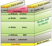
The n- and p-doped GaAs (100) 2o off toward [110] substrates were used. AlGaAs layers were grown at the temperature 650-750oC, growth rate 3 m/h and V/III ratio 65-100. The cells were fabricated with the following designs: 4.5x4.5 mm, 3.5x3.5 mm and 3.2x8.3 mm with 200 μm contact grid spacing. The contact grid shadowing was about 8%. Photolithography was used for front contact grid creation. The Au:Ge/Ni/Au and Ag:Mn/Ni/Au were thermally evaporated for n and p contacts respectively. The AlGaAs layers were used as back surface field (BSF) and wide bandgap window. The total thickness of the elements was 3 - 3.5 μm (Figure 1).
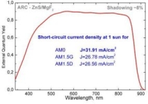
The investigations of the GaAs solar cells allow obtaining the high values of the photocurrent densities 31.91 mA/cm2 and 26.56 mA/cm2 for AM0 (1367 W/m2) and AM1.5D (1000 W/m2) respectively (Figure 2).
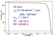
The active area photocurrent densities were about 34.68 mA/cm2 for spectrum AM0 and about 28.86 mA/cm2 for spectrum AM1.5. The terrestrial efficiency of 22.25% (Figure 3) was obtained at the 92 suns (AM0 spectrum). The measurements were carried out under Xe flash lamp.
The AlGaAs/GaAs solar cells with internal Bragg refector grown by low-pressure MOCVD have shown gains in efficiency and in radiation stability in comparison with standard AlGaAs/GaAs solar cells. The main reason of the degradation of photocurrent and efficiency in space solar cells is the reduction of minority carrier diffusion length upon electron or proton irradiation.
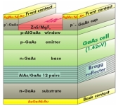
The radiation resistance can be increased by using of internal Bragg reflector (Figure 4). This allows to reduce the base thickness without losing of long wave sensitivity and decrease the influence of diffusion length degradation on the electrical parameters of the cells.
The grown structures consist of p-GaAs contact layer, p-AlGaAs window, p-GaAs (0.4-0.7 μm) emitter, n-GaAs (1-3 μm) base and Bragg reflector. The Bragg reflector consists of twelve pairs of AlAs/GaAs layers. The thicknesses of GaAs and AlAs layer in Bragg reflector were 59 nm and 72 nm.
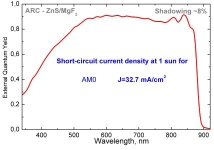
The existence of internal Braag reflector led to increase of photoresponse in the wavelength region of 800 - 900 nm(Figure 5). Photocurrent as high as 32.7 mA/cm2 for spectrum AM0 was achieved.
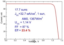
The outdoor measure-ments for the developed SCs have been carried ot as wel. The current dencity of 24.8 mA/cm2 under 893 W/m2 dirrect sun light irradiance has been measured. The efficiency of 23.4% was obtained at 17.7 suns for space spectrum AM0 (Figure 6). The conversion efficiency of 27.2% has been achieved for AM1.5D (893 W/m2)
It was demonstrated that knowledge of the Bragg reflector role as a back surface potential barrier and selective mirror in connection with cell internal structure parameters allows increasing the radiation resistance of GaAs solar cells. Reducing the base thickness to 1.1-1.5 μm and the base doping level to ND=1x1015cm-3 in GaAs cells with internal Bragg reflector allowed achieving a record-breaking EOL efficiency of 15.8% upon exposure to 3MeV electrons with 1x1015 cm-2 fluency.
The multi-junction solar cells grown by MOCVD have been investigated in our laboratory since 2004, when new R&D MOCVD installation AIX 200/4 was installed. The n on p and p on n structures of dual-junction GaInP/GaAs solar cell monolithic structures was grown by the MOCVD technique. The investigations of triple-junction monolithic structures on Ge substrate were begun.
GaInP/GaAs tandem cells.
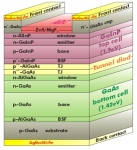
The GaInP/GaAs dual-junction solar cells structure were grown in the AIX 200/4 reactor. The n and p-doped GaAs (100) 2o off toward [110] wafers were used. The trimethylgallium trimethylindium trimethylaluminum and phosphine were used as main elements precursors for Al-Ga-In-P system.
The AlGaAs layers were used as back surface field and window for bottom GaAs cell. The p+-GaInP and AlInP were used in the top GaInP cell. The using n++-GaAs/p++-AlGaAs tunnel diode allows to provide electrical connection between GaInP and GaAs cells.
The solar cells were fabricated with the following designs: 3.5x3.5 mm and 3.2x3.8 mm with 200 μm contact grid spacing. The average shadowing was about 8%. The ZnS/MgF2 anti reflection coating was used. The Au:Ge/Ni/Au and Ag:Mn/Ni/Au were used as metallic contact to n- and p-doped GaAs.
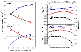
Investigations of dual-junction GaInP/GaAs SCs allowed to fabricate current matched structures for the AM0 and AM1.5D spectra and to obtain high efficiency for both terrestrial and space spectra.
The maximum value of the solar conversion efficiency of the manufactured dual-junction GaInP/GaAs SCs has been 30.03% (AM1.5D, 40 suns). For the SCs optimized for the space spectrum the efficiency has been 26.5% (AM0, 30 suns). (Figure 8).
The main research directions at the moment are:
- GaInP/GaAs monolithic dual junction concentrator solar cells for space and terrestrial applications;
- GaInP/GaInAs/Ge monolithic triple junction concentrator solar cells optimized for AMO and AM1.5 spectra;
- GaInP/GaAs mechanically stacked with GaSb triple junction concentrator solar cell for terrestrial applications
- GaInP/GaInAs/Ge mechanically stacked with InGaAsSb quadruple junction solar cells
